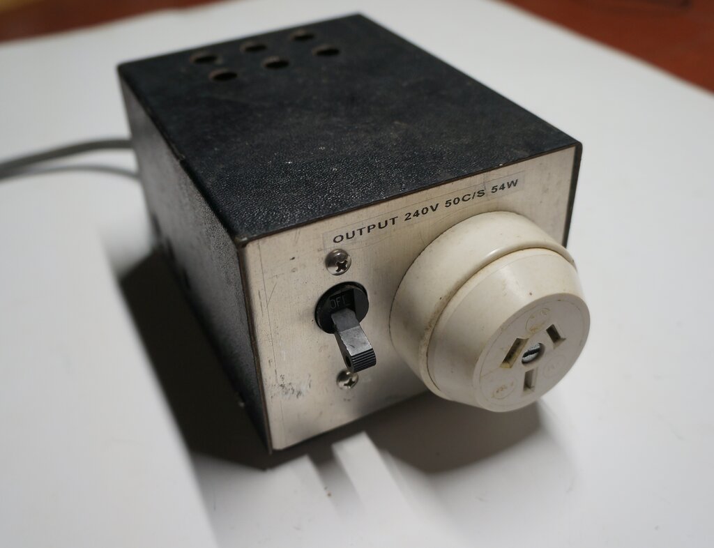
This inverter is a rebuild of an old project
which goes back to the late 1990's. It was a 12 to 240V inverter using
a Tandy 9-0-9V 3A transformer, which was switched by a pair of MJ3001 Darlington
transistors. The transistors were driven by a 4009 wired as an oscillator.
However, its performance was not the greatest
with regards to regulation, and the method of generating the switching
waveform was problematic with an unstable duty cycle. Furthermore, the
input current was rather high with no load.
For some time, thoughts were to use a
proper switchmode IC with push pull outputs and with pulse width regulation.
Typical of such IC's is the TL494 and SG3524. These IC's are normally used
in high frequency switchmode power supplies, but there didn't seem to be
any reason they couldn't work at 50c/s. The TL494 has been described in
this Model
T Ford voltage regulator.
Experiments were done with an SG3524,
since I presently have more of these than TL494's, and 50c/s operation
was proven to be possible. No doubt, a TL494 could be adapted for the following
design, since both these IC's are similar in a lot of ways.
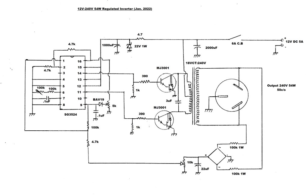
A circuit was assembled on a breadboard
and optimised. It was then built on Veroboard and installed in the inverter.
The SG3524.
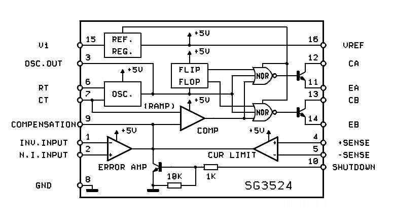
The SG3524 operates from 8 to 40V; this
supply being fed into pin 15. A 5V reference is available at pin 16. The
SG3524 has also been mentioned with regards to the Fun
Projects Voltage Regulator.
Oscillation frequency is set by the resistor
and capacitor at pins 6 and 7. Two output transistors are used to drive
the output circuit in push-pull, or if they are paralleled, in single ended
mode. These transistors can be used as emitter followers or as open collector
output..
To vary the pulse width for regulation,
two error amplifiers are provided. Pins 1 and 2 are used for voltage regulation
in the normal way, with pin 1 being fed a reference voltage, and pin 2
a sample of the output voltage. A second error amplifier is used for current
limiting; its inputs being pins 4 and 5. The error amplifier output can
be forced low by taking pin 10 high.
Oscillator.
The SG3524 is set to oscillate at 100c/s
by the .1uF at pin 7 and the resistance at pin 6. This is adjustable from
100k to 200k, for setting the exact frequency. The push-pull output divides
this in half; i.e., 50c/s.
The output transistors in the SG3524 are
used as emitter followers, with their collectors fed from the positive
supply. Their emitters drive the output transistor bases via 390R resistors.
1k load resistors ensure the transistors are off when there is no base
current.
Error Amplifier.
The Vref. of 5V at pin 16 is divided down
to 2.5V by the two 4.7k resistors at pin 2, which is the non-inverting
input of the error amplifier. The reason why 2.5V is used and not 5V, is
because the common mode input voltage is restricted to 1.8 to 3.4V.
Output of the error amplifier is at pin
9. The gain of the error amplifier is set to 21 times by means of the ratio
of the 100k and 4.7k connected to the inverting input at pin 1. If the
voltage at pin 1 increases beyond 2.5V, the output at pin 9 goes low, which
reduces the pulse width of the oscillator. The .1uF at pin 9 is for stability.
There is a second error amplifier with
inputs at pin 4 and 5. Its output is in parallel with that of the other
error amplifier. It can be used as a current limiter, by measuring the
voltage drop across a low resistance in series with the emitter supply
to the output transistors.
This was not done because there wasn't
enough space to add the extra components, and the inverter already had
a 6A circuit breaker for overload protection.
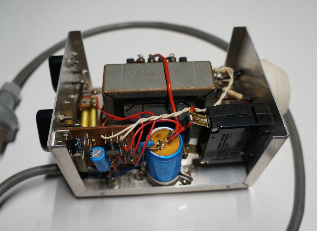
Most of the circuit is built on a piece of Veroboard.
Regulation.
The AC output is divided down and rectified
by means of the two 100k 1W resistors and the bridge rectifier. The resultant
DC is filtered by a 22uF capacitor and applied across a 10k trimpot. This
becomes the source of the error voltage. As the AC output rises, so does
the DC across the trimpot (which is roughly around 10V). A portion of this
is fed back into the error amplifier, and so the pulse width is reduced,
which in turn reduces the output voltage. The 100k's are 1W not because
of power dissipation, but to get the required voltage rating. The rectifier
could be connected directly to the AC output, with the 200k resistance
on the DC side, but connecting it as shown reduces the voltage stress across
the rectifier diodes.
Unfortunately, because of the output waveform
shape, this method of measuring the output voltage is not completely accurate,
but is adequate for a simple low power inverter.
The astute reader may notice that the 22uF will take a short period of time to initially charge when the inverter is first switched on. This means the output will be unregulated for this time. A soft start circuit would eliminate this, but was not included because of lack of space. The unregulated voltage only appears for about a second and is not excessive.
Output Transistors.
These are MJ3001's, a Darlington power
transistor in a T03 case. Internally, there is also a diode between the
collector and emitter, and there are also internal base resistors. The
transistors are rated at 10A and 80V which suit this kind of circuit well.
Being Darlington, the saturation voltage is higher than desirable, but
they are easy to drive in view of their high current gain (1000 x).
It is not known what the diode ratings are. These days, MOSFET's are much
preferred and would be my choice now, but this inverter was originally
built when such devices were new and expensive.
Aluminium case provides sufficient heatsinking for the output transistors.
Transformer.
This is a 9-0-9V 3A to 240V type once
sold by Tandy Electronics in the 1980's. It started life with a vibrator
inverter I built in 1983, but this was dissembled in the early 90's. The
transformer was then used in a transistor self oscillating circuit, but
while simple, was very inefficient with the base resistors getting very
hot. I now suspect the 2N3055's used had an unusually low gain. The inverter
was then modified to use the separate oscillator using a 4009 referred
to previously.
The power rating is 18 x 3 = 54W. These
days, I would use a toroid in preference, since efficiency and regulation
are superior.
First Test.
The inverter worked well except there
was some concern about spikes appearing at the transistor collectors. With
spikes included, the voltage across the primary was around 160Vp-p. This
is just within the ratings of the MJ3001's with their 80V collector voltage.
Since this is not good design to leave
it like this, corrective measures were taken. Capacitance across the primary
improved things markedly, with 3uF reducing the spikes to around 90Vp-p.
I used two paralleled 1.5uF 400V polycarbonate capacitors. Current consumption
also dropped slightly due to the capacitor's tuning effect. However, it
was found that when the inverter was fully loaded, the spikes were of excessive
amplitude again.
Dead Time.
Since the spikes appeared only under heavy
load, it was clear that this was when the inverter was out of regulation,
and the duty cycle was 100%. A possibility was that both output transistors
were on at the same time, for a short period at the switching point. The
SG3524 does not have a dead time control pin, but the data shows a simple
circuit for limiting the duty cycle if required. This uses a diode clamp
at pin 9, which is the error amplifier output. A 5k trimpot connected across
the Vref. supply provides a variable voltage to set the diode conduction
point. For example, if the trimpot wiper is set to 2V, pin 9 cannot go
above 2.6V (the 600mV being of course the junction voltage of the diode).
I used a BAV19 since I had one to hand, but obviously a 1N914 is also suitable.
This worked well, and the trimpot could
be adjusted just so the spikes disappeared when the inverter was running
fully loaded. Alternatively, it was found that slowing down the output
transistor switching speed achieved the same result. Since there was just
enough room to mount the parts, the adjustable dead time circuit was used
in preference. It was felt that the switching would be more rapid, and
result in less transistor dissipation, than if capacitors were used to
slow down the switching. For anyone wanting to try capacitors, the optimum
value was 0.39uF from base to emitter.
Supply.
The incoming 12V supply is fed via a 6A
circuit breaker for overload protection. It will also trip if the polarity
is reversed, by virtue of the diodes in the MJ3001's conducting. The SG3524
supply is clamped to a maximum of 22V with a zener diode, should there
be spikes on the supply. The 4.7R limits the current if the zener should
conduct. Connection to the 12V supply is by a two pin polarised plug.
| Load | Output Vrms | Input current 12.6V | Pulse Width |
| No load | 255 | 640mA | 64% |
| 15W incandescent | 240 | 1.9A | 77% |
| 25W incandescent | 235.5 | 2.45A | 85% |
| 40W incandescent | 227.5 | 4.3A | 92% |
| 53W incandescent | 215 | 5.35A | 94.5% |
| 15W fluoro LPF | 238 | 4.65A | 99% |
The inverter was tested for regulation and current consumption. Input was maintained at 12.6V at the input of the supply cable. Regulation starts to run out at around 40W. This is partly because of the transformer design, and also the relatively high saturation voltage of the MJ3001's. Various incandescent lamps were used as a resistive load. A 15W fluorescent lamp with low power factor was also tested. It drew 4.65A from the 12.6V supply, which is very high at 58W. This is an extremely inefficient way to use a fluorescent lamp and is not recommended. A 20W fluorescent lamp with power factor correction was also tested. It drew 5.4A (68W).
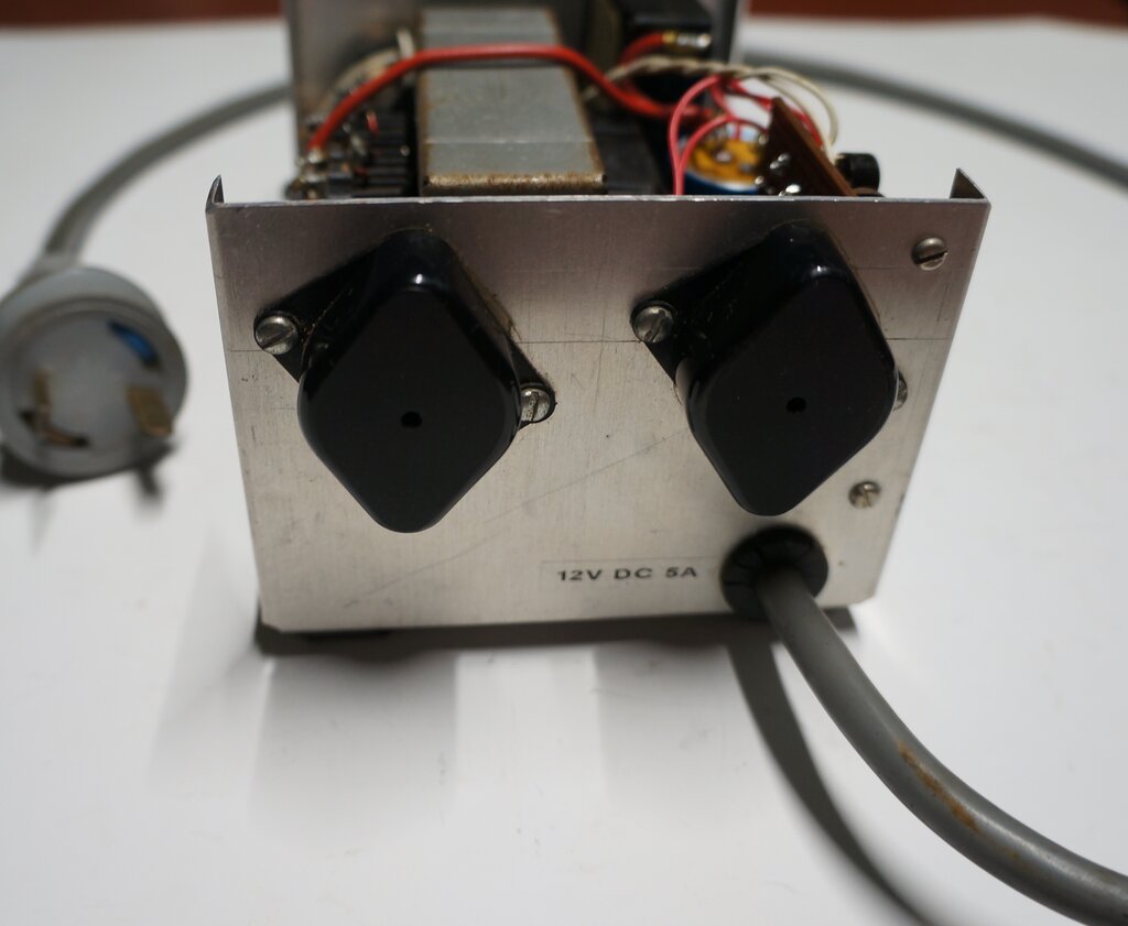
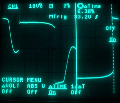
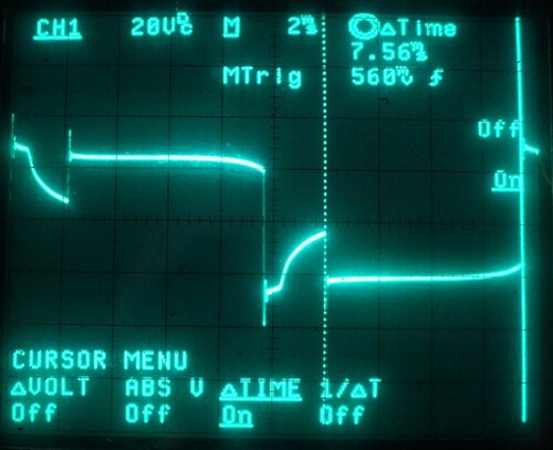
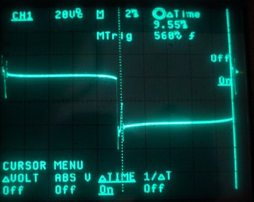
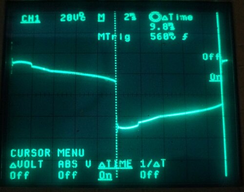
Primary Waveforms.
The oscilloscope was connected across
the full primary to obtain the following waveforms. The pulse width variation
with different loads can clearly be seen.
No load and 15W waveforms.
25W and 53W waveforms.
15W fluorescent lamp with no power factor correction.
Improvements.
If this inverter was to be built from
the beginning again, I would use a toroidal transformer. As it is, the
transformer runs warm under full load, and the 640mA no load current is
rather high. This illustrates that not all transformers work efficiently
in reverse. I suspect that the transformer does not have enough primary
inductance (and is therefore saturating at the high duty cycle). As I recall,
the no load current was lower when it was used at 100c/s with a vibrator.
MOSFET's would make a better switching
device than the transistors, which would improve regulation and run cooler.
The current sense facility would be worthwhile, since it would avoid having
the circuit breaker trip during an overload. Also, it would allow a definite
overload point to be set, something not possible with a thermal circuit
breaker. On that point, using a circuit breaker as a main switch is not
always desirable, since continual flexing of the internal copper braid
eventually causes it to fail. A soft start circuit should also be included,
especially for higher power versions. Use could also be made of the shuntdown
pin for a thermal overload.
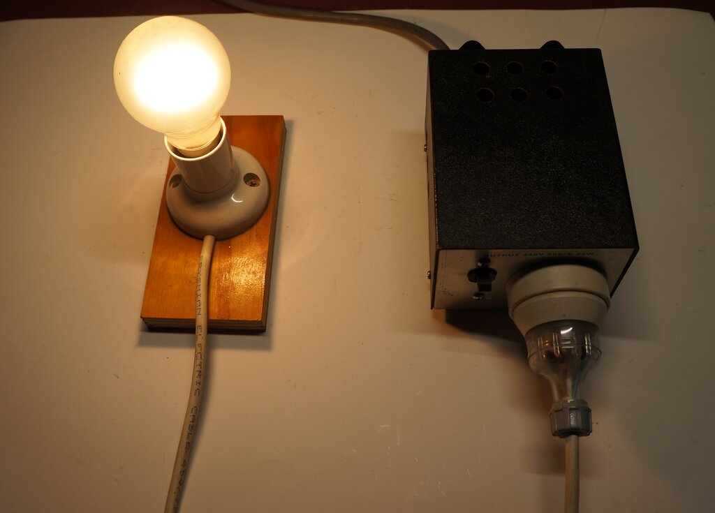
Inverter powering 25W light bulb.