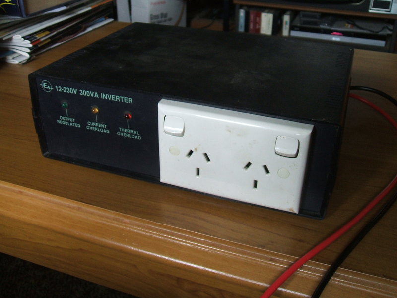
The 1985 model is housed in a compact low profile case.
The 1985 model is housed in a compact low profile case.
This was the third in line of 300W inverters
presented by Electronics Australia. It appeared in the September 1985 issue,
and was an update of the June 1981 version. This in turn was an update
of the original February 1979 design which was developed by a reader from
New Zealand.
The 1985 model was a departure from the
earlier designs in that it was the first to use a toroidal transformer,
and to have everything mounted in a low profile plastic case. Additionally,
it incorporates automatic start.
The toroidal transformer improves efficiency as well as making for
a lighter, more compact, unit.
This particular inverter came to me via
the HRSA for next to nothing. As a collector of inverters I just had to
have it. It was obviously a kit, although one kit supplier, Altronics,
did sell made up versions. As this inverter did not have the Altronics
name on the front panel I could tell it wasn't their kit. It wasn't the
DSE kit either, as reading through their instructions it mentions a steel
base plate, which this didn't have - it's aluminium. That pretty much narrows
it down to Jaycar.
The constructor had done a good job of
building it, but there were a few things I wasn't happy about. Also, the
inverter was faulty.
The Circuit:
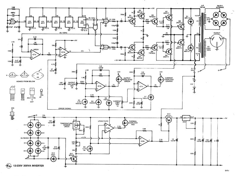
For the most part the circuit is largely
the same as the previous models, but the 1985 model has included an automatic
start circuit.
The timebase uses a 4MHz crystal which
is divided down to 100 Hz by means of cascaded 4017 divide by 10 counters.
This means that unlike many other inverters, using RC time constants or
vibrators, clocks will maintain accuracy, and synchronous motors will always
run at the correct speed. The short term frequency stability of this inverter
is actually better than the mains supply.
The anti phase 50Hz signals come from
IC1b,c, and d. From here, they proceed to the push pull amplifiers and
output stages via 1uF capacitors. Capacitive coupling means that if the
timebase stops, the output stage won't be turned on permanently, possibly
destroying the output transistors.
The 100K/150pF networks slow down the
switching of the output stages very slightly, so that opposing pairs of
output transistors can never be switched on at the same time, as might
happen if their switch off is too slow.
From here, the signal is buffered by the
Darlington pairs Q1/Q3 and Q2/Q4. The output stages are also connected
as Darlington pairs with TIP3055's driving parallel connected 2N3771's.
To ensure equal current sharing in the output transistors, 0.1R base resistors
are used.
The output transistors are protected against
back EMF by means of 10A diodes, type MR110. These diodes also provide
reverse polarity protection, conducting if the 12V supply is connected
in reverse, thus blowing the 30A fuse.
Regulation.
A feature of these EA designs is the pulse
width regulation of the output. Many inverters simply have a tap changing
switch for the power transformer secondary (such as the Radar
described here). This leaves it up to the user to work out what tapping
to use, which of course might not be optimum. Furthermore, the output is
still not actually regulated - the optimum tap selection being for a certain
input voltage and a certain load.
In the EA designs, a 12V secondary winding
provides a feedback voltage, proportional to the output. It's fed into
an error amplifier which then reduces the pulse width of the drive, or
increases it as necessary, so that the output remains at 240V.
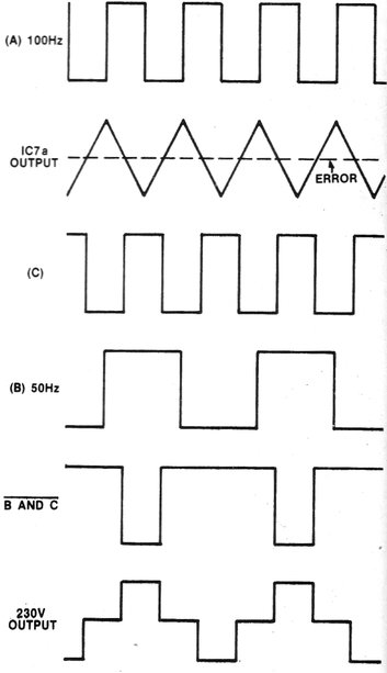
These waveforms help explain the operation.
IC7a is a triangle wave generator. It integrates the square wave to convert
to a triangle wave. The triangle wave is fed into the inverting input of
IC7d. As the triangle wave is synchronised to the timebase (waveform A),
it can be seen that as the voltage at the non inverting input is varied,
the pulse width at pin 14 (waveform C) will vary.
The 12VAC from the transformer is rectified
and filtered, producing DC proportional to the output voltage. A sample
of this is taken from the wiper of VR1 and compared with a 5.6V zener diode,
using IC7b. If the output voltage is too high, pin 7 goes low, pulling
down pin 12 of IC7d and thus reducing the output pulse width.
The output peak voltage is dependent on
the battery voltage, transformer regulation, and transistor saturation
voltage. It is not regulated, therefore. However, by varying the width
of the waveform, the rms voltage can be regulated. It is the rms that determines
the power fed into resistive loads, like heating elements and incandescent
light bulbs. Peak voltage affects loads where a DC supply is used. This
is because the filter capacitors charge up to the peak voltage.
Current Overload protection.
Unlike simple designs relying on circuit
breakers or fuses, if this inverter is overloaded it will simply limit
the output to 300W. Output current is sensed through a low value emitter
resistor R1, which in this situation is 20cm of 1mm wire. The voltage across
this is fed into IC7c and compared with a voltage reference adjustable
from 0 to 600mV. Pin 8 of IC7c will go low if the voltage across R1 is
greater than the fixed voltage reference at the non inverting input. D6
and D7 function as an OR gate so that the pulse width is reduced for both
or either excess current or excess voltage.
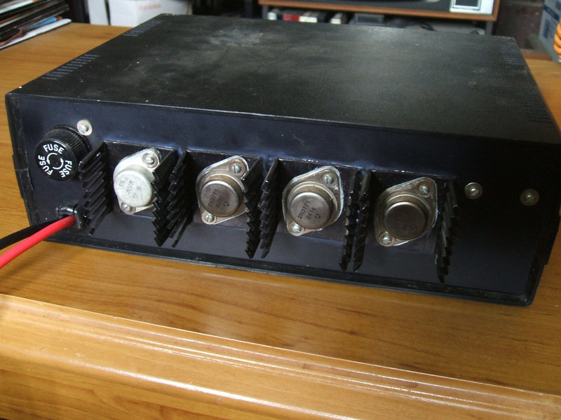
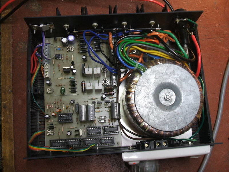
Back of inverter shows the 2N3771 transistors. The back panel is
metal which helps with heat dissipation.
Thermal Overload.
Because a prolonged current overload will
cause the output transistors to overheat, temperature sensing of the heatsinking
is provided for. In the earlier designs, the leakage of a germanium transistor
was used to detect this, but by 1985 such devices were seen as outdated.
Instead, an LM334 temperature sensor is used. Connected to a resistive
voltage divider, the voltage at the V- pin will change with temperature.
This is compared to the voltage across a 5.1V zener diode (D3) and if it
is higher, pin 7 of IC8b goes high. This causes Q12 (BC337) to switch off,
depriving the timebase of supply. The timebase supply is regulated at 9V
by the LM317. The over temperature shut down is set for 70 degrees C on
the 2N3771's.
Auto Start.
The circuit here is based on that submitted
by a reader in 1980 for the 1979 inverter. Interestingly this wasn't mentioned
in the 1985 article, possibly giving the incorrect impression that EA came
up with the idea themselves. Basically, when it senses a DC path through
the 240V load it switches on the 9V supply to the timebase.
Following the circuit, the 12V supply
is fed via a 22K resistor (near point B and the chain of diodes D13-D20),
through the load connected to the output socket, thence through the transformer
secondary and back down to point A. It can be seen therefore, that if a
load is plugged into the inverter, point A will have a positive voltage
present. Thus current will flow via D12 into the base of Q11. When this
happens, the collector goes low, completing the path for the negative supply
for IC8b, which then allows Q12 to switch on, and thus the inverter timebase.
To make it practical, several refinements are needed. Once the inverter
starts, there would 240V fed into the base of Q11 if it wasn't for the
string of diodes D13-D20. These clamp the voltage to about 1.5V. D12 forms
a half wave rectifier in conjunction with the 470uF so that Q11 still remains
on when the output polarity reverses every half cycle.
The 47uF bipolar electrolytic bypasses
stray capacitance in loads such as long extension leads or mains filters
in appliances, so that the inverter does not keep running when the actual
load is switched off. In other words, it bypasses most of the AC component
flowing through diodes D13-D16 in such circumstances.
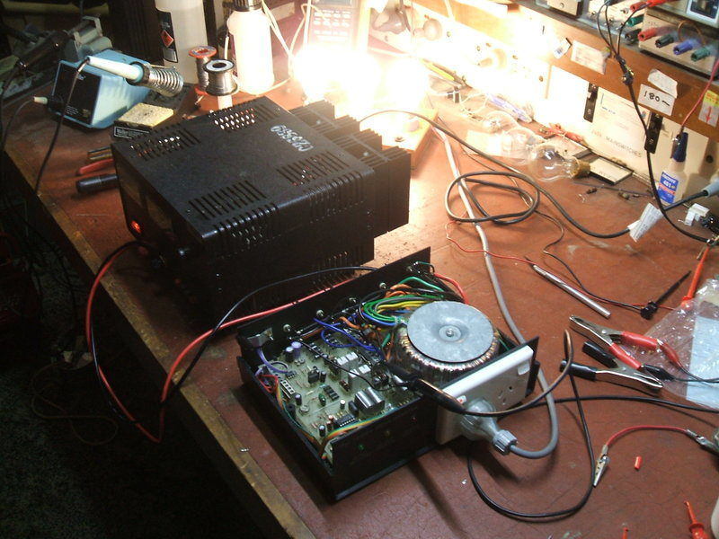
Here the inverter is on test, powering three 100W light bulbs. Power
source is a 30A 12V power supply.
First Observations.
The first thing noted was that one of
the 2N3771 output transistors had shorted. The constructor had attached
about 5m of what looked like 1.5mm twin flex as the input supply cable.
Obviously that would have to go. There
is no way 30A can be drawn through such a long length of cable without
severe voltage drop, to say nothing of the inadequate wire gauge to start
with. The internal wiring was a little messy and could do with tidying
up. The earth connection to the double power point hadn't even been connected.
Not so elegant was the earth connection to the back panel - the wire had
been soldered to one of the nuts securing the LM334, rather than using
a lug.
I also noticed the corner of the baseplate
had been squashed down deliberately. It appears this was getting in the
way of the cable clamp grommet for the supply cable.
Getting it going.
As a temporary measure, knowing I wasn't
going to draw full output yet, I simply disconnected the shorted 2N3771.
Alas, this wasn't enough - the auto start wasn't working properly at all.
To cut a long story short, D12 had shorted, IC8a was faulty, and so was
Q12. One has to wonder if this was associated with the failure of the 2N3771
and what kind of fault would cause this. One thing I don't like about this
auto start circuit is that Q11 has no current limiting to its base. If
D13-D16 are fully biassed on and 1.5V is present, then the base emitter
junction of Q11 and D12 have to absorb this voltage. With the Vbe of Q11
being 600mV, that would mean 900mV being forced across D12 - a germanium
diode, which should only have 250mV across it. To overcome this bad design
fault, I included a 150R resistor in series with diode. That should prevent
any future failure.
Having done that. the inverter came to
life, powering a 15W bulb quite nicely, and the auto start was working.
I replaced the defective 2N3771.
Tidying it up.
At this point I decided to tidy up the
wiring. The transformer was rotated slightly so its wires weren't covering
the top of the PCB. Instead of the multiple flexible wires going to the
2N3771 emitters, I replaced that with one length of tinned copper wire
- much neater. I also tidied up the collector and base wiring - unknowingly
making a mistake!
The long twin flex supply cable was replaced
with red and black 1m lengths of 25A cable.
I also took the opportunity to provide
reverse polarity protection to the auto start and timebase supply circuits.
Looking at the circuit, we can see there is none.
Simply by taking the 12V feed from the
transformer side of the 30A fuse we get our reverse polarity protection
by virtue of the 10A diodes conducting and blowing the fuse.
Upon powering up again, all seemed good
except for the TIP3055's getting hot enough to smoke and burn fingers.
This seemed odd because they shouldn't be carrying anything more than the
2N3771 base current. After destroying three TIP3055's, I realised what
the problem was. I'd cross connected the Darlington pairs! What this meant
was the TIP3055's were actually working as the output transistors, with
the base emitter junctions of the 2N3771's merely completing the emitter
circuit of the TIP3055's. It also explained why the output voltage dropped
severely above 75W output.
Having fixed that up, full 300W output
was available without anything untoward happening. I used a true rms meter
to set the output voltage to 250V with a 15W load. This drops to about
225V with 100W, and then to about 185V at 300W. I can only put this down
to the transformer because the supply voltage was maintained up to the
transformer centre tap, and the saturation voltage of the output transistors
was the specified 2V at that current.
Our constructor had not attempted to set
the current limit trimpot (probably why the damage occurred). It was set
at maximum. So, I set it with a 300W load just until the over current protection
came in and backed it off slightly.
The over temperature setting was then
adjusted so that the inverter shut down when the output transistors became
rather warm to the touch.
Performance and limitations.
The worst aspect of the original EA 300W
inverter design was its inability to deal with low power factor loads.
Induction motors and fluorescent lamps without phase correcting capacitors
simply would not work. This was carried through to the 1985 version. The
problem is with the regulation circuit not sensing rms properly. I had
noticed that the later Altronics versions didn't seem to have the same
problem, and a close look at the circuit showed the difference. The 1M
resistor in the feedback path of IC7b had been changed to 1.8K, reducing
the gain of the error amplifier substantially. I then found a note in EA
for February 1986 stating that this resistor should be changed to 680R.
This kit must have been purchased after
February 1986, because this resistor in this inverter was 680R.
The change of resistor helps quite a lot,
but is still not the perfect answer.
It was also stated in the February 1986 notes that the heatsinking was found to be inadequate. They claimed that it was only good enough for 200W continuous. 300W could only be drawn for about 25 minutes before overheating. They also admitted the lack of reverse polarity protection I mentioned above. One has to wonder how thoroughly the prototype was tested in real world conditions.
A limitation of the auto start circuit
is that it won't work with certain loads that appear as open circuit, or
very high resistance, until they're powered up. A good example is a fluorescent
lamp. The subsequent model of inverter, redesigned by Altronics, incorporates
a manual bypass switch to overcome this.